


NanoTechnology Center
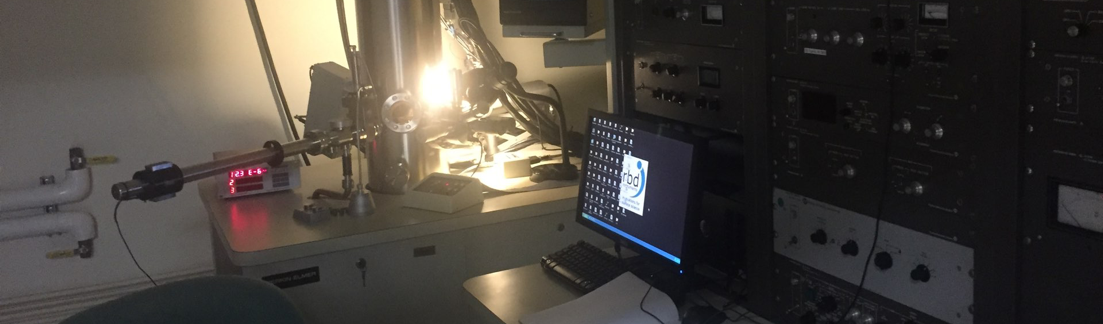
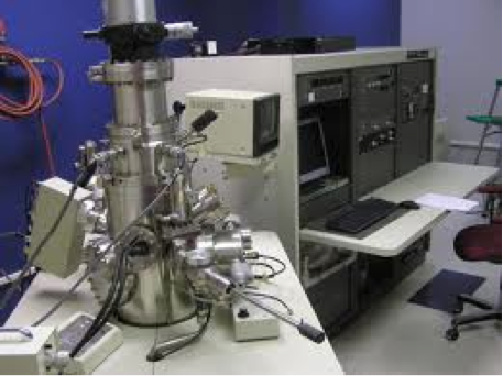
Auger/XPS

PHI Scanning Auger and XPS system
X-Ray Photoelectron Spectroscopy (XPS) Surface Analysis / ESCA and Auger Electron Spectroscopy (AES)
Company Description:
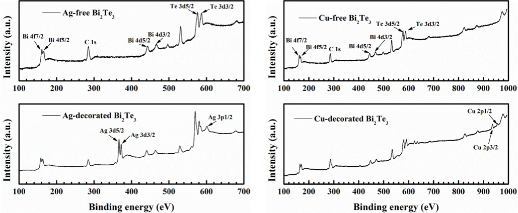
X-ray Photoelectron Spectroscopy (XPS)... What is X-ray Photoelectron Spectroscopy (XPS)? XPS, also known as ESCA, is the most widely used surface analysis technique because of its relative simplicity in use and data interpretation. The sample is irradiated with mono-energetic x-rays causing photoelectrons to be emitted from the sample surface. An electron energy analyzer determines the binding energy of the photoelectrons. From the binding energy and intensity of a photoelectron peak, the elemental identity, chemical state, and quantity of an element are determined. The information XPS provides about surface layers or thin film structures is of value in many industrial applications including: polymer surface modification, catalysis, corrosion, adhesion, semiconductor and dielectric materials, electronics packaging, magnetic media, and thin film coatings used in a number of industries. Auger Electron Spectroscopy (AES)...
What is AES? Auger Electron Spectroscopy (AES) is an analytical technique that uses a primary electron beam to probe the surface of a solid material. Secondary electrons that are emitted as a result of the Auger process are analyzed and their kinetic energy is determined. The identity and quantity of the elements are determined from the kinetic energy and intensity of the Auger peaks. The nature of the Auger surface analysis process is such that Auger electrons can only escape from the outer 5-50 Å of a solid surface at their characteristic energy. This effect makes AES an extremely surface sensitive technique. A finely focused electron beam can be scanned to create secondary electron and Auger images, or the beam can be positioned to perform microanalysis of specific sample features. Applications include materials characterization, failure analysis, thin film analysis, and particle identification for semiconductor and thin film head manufacturing.
Training is required to use this instrument. For training schedules and access contact the facilities manager or director: carroldl@wfu.edu
The Nanotechnology Center 2019