

Microscopy
These facilities have been made possible through a generous grant from the DataMax Foundation


NanoTechnology Center

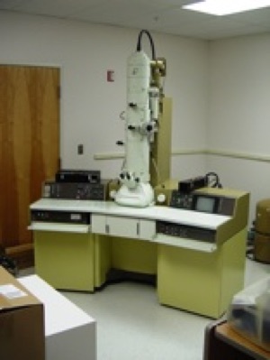
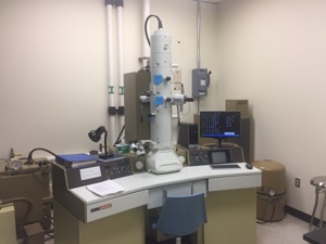
300 kV TEM:
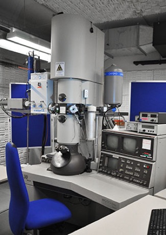
Our Philips (FEI) CM 30, 300 kV microscope is the workhorse of our intermediate-resolution characterization. The machine has been highly modified with new cameras, operational software, and other additions to improve: imaging, diffraction and analytical techniques at high spatial resolution and detection efficiency. The upgraded high resolution digital camera is coupled with a number of analytical software packages that allow for on-site or off-site data work. Analytical capabilities are provided by an Oxford Instruments EDAX system. The system is particularly suited for materials science, embedded structures, interfaces, matrix composites etc.
-
1.High-resolution bright- and dark-field imaging
-
2.Small-probe convergent beam (<2nm)
-
3.Large specimen tilt compatible with high resolution
-
4.Point-point resolution: 0.2 nm
-
5.Line resolution: 0.2 nm
Access to this microscope requires training and sign-off by the facilities manager. We recommend that users take the Advanced Imaging class or equivalent before actual training on the microscope begins
120 kV TEM:
Our JEOL 1200 EX is an easy-to-use TEM ideal for lower resolution materials science and biological samples. This workhorse microscope features a double condenser projection lens, 60-120 kV, bright/dark field imaging, electron diffraction, eucentric goniometer (60° tilt). A newly installed high resolution digital camera provides multiple file outputs and makes image capture easy.
-
1.Resolution 0.45 nm point to point
-
2.300,000X magnification
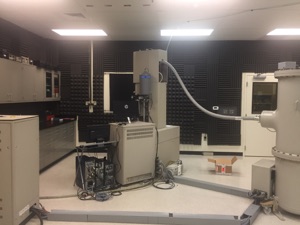
Field Emission SEM:
The JEOL 6330 is a cold field emission scanning electron microscope. Cold field emission scopes have the advantage of high brightness (large current density) and small beam diameter (high resolution) at low accelerating voltages to allow imaging of soft polymeric materials without causing sample damage. Resolution of the instrument is around 15 Angstroms depending on the sample. This instrument is soon to be upgraded with an energy dispersive X-ray spectrometer (EDS) for elemental analysis, a backscattered electron detector that allows compositional analysis, and a cathode luminescence detector that can image complex, characteristic-visible spectra for detailed molecular structure information.
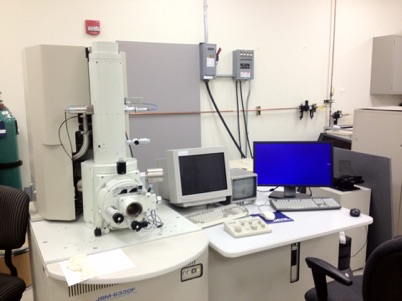
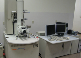
Access to this microscope also requires training and clearance. However, this system is particularly easy to align and use with sample turn around taking minutes typically.
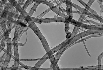
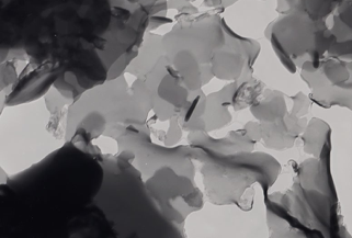
Image Gallery
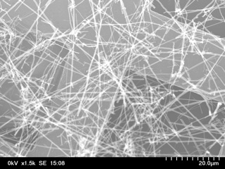
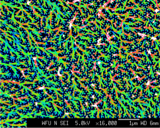
(left) GaN nanowires grown by CVS and imaged with the FE-SEM. The substrate is a TEM grid. (right) Silver nanowires that are hyperbranched to form “gecko feet.” False color image from the FE-SEM imaging software.
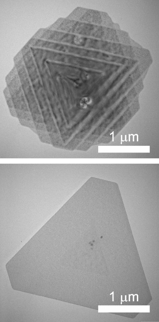
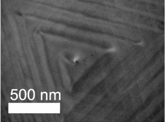
Single nanosheets (atomically thin) of VOx.
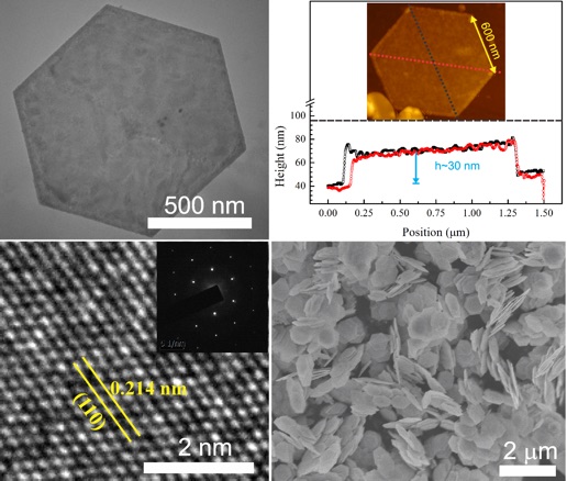
multiwalled carbon nanotubes

The Nanotechnology Center 2019