


NanoTechnology Center
Scanning Probes

Atomic Force Microscopy:
(Description from the JEOL web site)
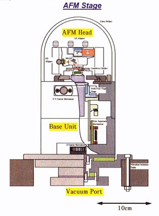
The JSPM-5200 is a multipurpose, high resolution SPM offering ease of use with diverse measurement and sample environments. The JSPM-5200 can be used in various native environments -- from ambient air, controlled atmosphere, fluid, or vacuum, with the sample heated to 500° C (773K) or cooled to -143° C (130K). The can also perform a wide range of applied measurements including the combination of image signals and instantaneous switching between operation modes. The open architecture of the JSPM-5200 provides multiple access ports and easy access to the probe. The JSPM-5200 can be configured as either an atomic force microscope (AFM) or scanning tunneling microscope ( STM ) by merely changing the tip. STM modes include CITS, I-V, S-V, and I-S. Standard AFM modes include contact, friction force microscopy, current image, non-contact and discrete contact with either slope detection or frequency detection, and phase imaging. A patented drift-free stage is implemented to provide an extremely stable imaging platform.
Scanning Tunneling Microscopy:
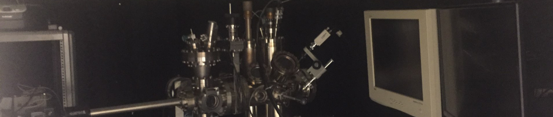
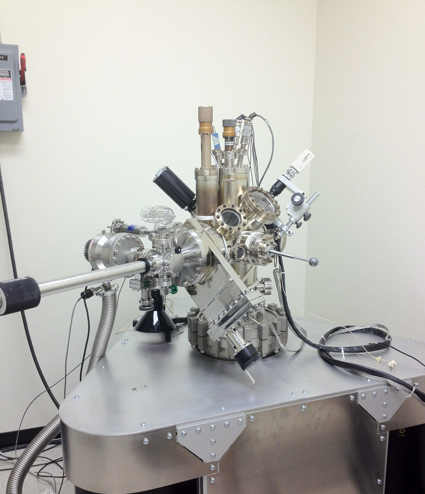
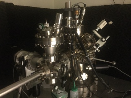
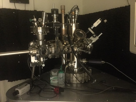
This microscope was developed in cooperation with RHK Technology, Inc. It is equipped with a cryostat modified to reduce inherent "bubbling" vibrations. The ultra high vacuum system was custom designed and built by Duniway Stockroom Corp. The vibration isolation system is an 'in-house' design and utilizes a custom Newport air suspension system. The STM is based on a "Besoke" scanner, flow LHe cryostats and sealed heating filaments for temperature control down to 20 K (for now) and up to 1000 K. It is specifically designed to collect images and perform variable-gap tunneling spectroscopy simultaneously. Further, we typically use quite low tunneling currents with imaging having been achieved at tunnel currents below 1 pA. The system is ideal for studies of nanostructures which might otherwise be damaged by the large field densities within the tunneling junction. Modifications are constantly being made to this machine as we develop new techniques for high precision determinations of electronic phenomena in nanostructures.
The system is installed in its own sound proof room, isolated from the rest of the laboratory.
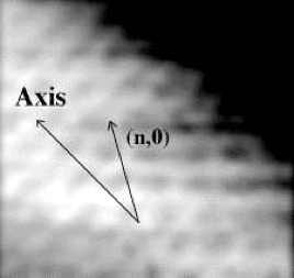
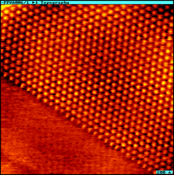
(left) STM image of a LB film on graphite. Registry with the atomic lattice below the film can be seen. (right) atomic resolution of a single walled carbon nanotube taken with the RHK.
The Nanotechnology Center 2019
STM lab